



Advanced Optical Sorting Systems in Electronic Component Manufacturing
2025-07-01 22:43Advanced Optical Sorting Systems in Electronic Component Manufacturing
Precision-Driven Quality Control for MLCCs, LTCCs, ICs, and Ferrite Cores
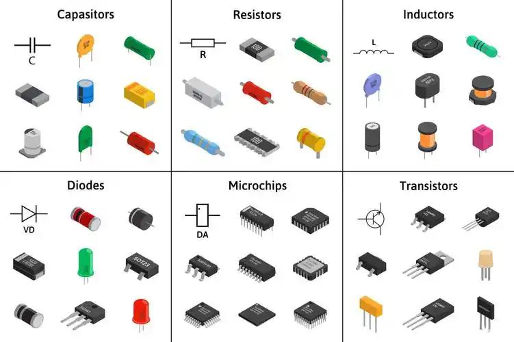
I. Industry Challenges & Technological Imperatives
Electronic component manufacturing demands micron-level precision across high-volume production. As depicted in the provided image, miniature multilayered ceramic capacitors (MLCCs), low-temperature co-fired ceramics (LTCCs), chip-scale resistors/inductors, ICs, and ferrite cores require defect detection capabilities beyond human vision limits:
Tolerance Thresholds: MLCC electrode misalignment <5μm
Critical Defects: LTCC micro-cracks ≤20μm
Throughput Needs: SMD component sorting at >30,000 UPH
Optical sorting machines address these challenges by integrating hyperspectral imaging, deep learning, and robotic automation to replace error-prone manual inspection.
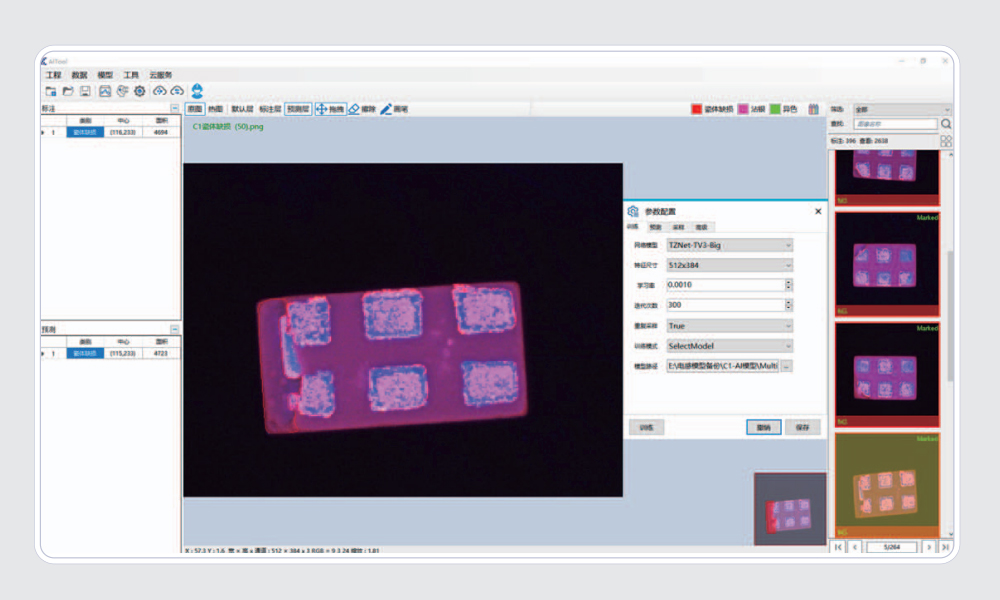
II. Component-Specific Optical Sorting Architectures
1. MLCC/LTCC Ceramic Components
Defect Detection:
? Surface pits/scratches → 5MP coaxial darkfield imaging
? Delamination → Terahertz wave subsurface tomography
? Electrode bleed → Color variance analysis (ΔE<0.1)Dimensional Verification:
? Laser triangulation for thickness (±2μm accuracy)
? Edge chipping detection via polygon-matching algorithms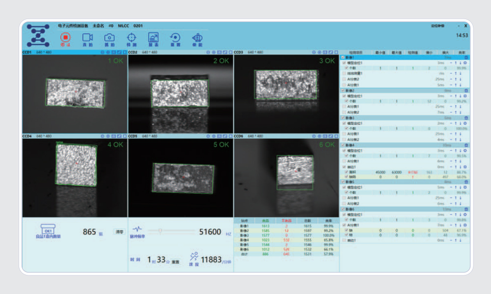
2. Chip Resistors/Inductors
Parameter Validation:
? Termination plating integrity → 20X optical microscopy
? Marking legibility → OCR with 99.97% read rate
? Coplanarity → 3D structured light (10nm Z-resolution)Performance Grading:
? TCR measurement via thermal imaging during stress testing
3. Integrated Circuits
Lead Frame Inspection:
? Pin coplanarity → Moiré interferometry
? Solder ball bridging → IR reflection analysis
? Wire bonding defects → 1μm-resolution X-ray laminographyContamination Control:
? Particulate detection down to ISO Class 3 standards
4. Ferrite Cores
(Image Reference: Bottom-left "Ferrite Core" section)
Material Integrity:
? Air gaps/cracks → Terahertz time-domain spectroscopy
? Dimensional accuracy → Shadow-free backlight metrology
? Coating uniformity → UV fluorescence imaging
III. Core Sorting System Technologies
A. Optical Subsystems
| Technology | Specifications | Component Applications |
|---|---|---|
| Hyperspectral Imaging | 400-1000nm range, 5nm resolution | Counterfeit material detection |
| Structured Light 3D | 5μm XY, 200nm Z accuracy | Solder paste height mapping |
| High-Speed TDI Camera | 32k lines/sec scan rate | Moving web inspection |
| Automated X-Y Theta | ±0.5μm positioning precision | Die attach verification |
B. AI-Driven Defect Recognition
Convolutional Neural Networks: Trained on >1M defect images
? Adaptive learning for new failure modes (e.g., tin whiskers)Anomaly Detection Algorithms:
? Unsupervised clustering for zero-defect validationParametric Correlation Engine:
? Relate optical defects to electrical performance (e.g., Q-factor degradation)
IV. Integration with Smart Manufacturing
1. Industry 4.0 Implementation
Equipment Interfacing:
? SECS/GEM protocols for real-time process adjustment
? FDC (Fault Detection Classification) integrationDigital Twin Simulation:
? Virtual sorting parameter optimization before physical runs
2. Automated Material Handling
Component-Specific Carriers:
? Vacuum end effectors for <1G acceleration shock
? Anti-static waffle trays with RFID tracking
V. Quantifiable Quality & Cost Benefits
| Metric | Before Optical Sorting | After Implementation |
|---|---|---|
| Defect Escape Rate | 820 PPM | 2.7 PPM |
| Inspection Speed | 5,000 UPH (manual) | 45,000 UPH |
| False Rejection | 18% | 0.3% |
| Rework Labor Cost | $18.50/kg | $1.20/kg |
Data Source: SEMI E178 global component manufacturing study
VI. Industry-Specific Case Studies
A. Automotive MLCC Production
Challenge: AEC-Q200 compliance requires 0 PPM cracks
Solution:
? Terahertz inline inspection with 99.999% coverage
? Multi-layer registration error detection <2μmOutcome:
? Achieved 0 field failures in 10M+ components
B. Medical IoT Chip Sorting
Challenge: Implantable device contamination control
Solution:
? ISO 14644-1 Class 4 cleanroom integration
? 0.1μm particulate monitoringOutcome:
? Passed FDA 21 CFR Part 11 audits with zero observations
VII. Standards Compliance
Electrical Testing: IEC 60384-1 (MLCCs), IEC 60195 (Ferrites)
Optical Calibration: ISO 5725 accuracy verification
Traceability: ASTM E2919 component-level data logging
VIII. Future Developments
Quantum Imaging Sensors: For sub-surface defect resolution beyond diffraction limits
Edge Computing Integration: Localized AI inference <5ms latency
Green Manufacturing: Sorting-guided material recovery (>95% precious metal reclamation)
Conclusion
Optical sorting machines have transformed electronic component manufacturing into a data-driven science. By deploying component-specific optical architectures as depicted in the image—from MLCC delamination detection to ferrite core structural analysis—manufacturers achieve unprecedented levels of quality assurance while reducing costs. The convergence of multi-modal imaging, Industry 4.0 connectivity, and adaptive AI ensures that optical sorters will remain pivotal in enabling next-generation electronics scaling, particularly for 5G, automotive electrification, and industrial IoT applications.
Related product and article resources
For procurement comparison and technical evaluation, readers can continue with these related product pages and supporting articles.
- Products
- Product catalog
- Contact the sales team
- Contact us
- AI Optical Sorting Machine Supplier Evaluation Guide for Overseas Buyers
- AI-Powered Vision Inspection: How Machines Are Redefining Zero-Defect Manufacturing
- The working principle of an external appearance inspection device
- Are There Environmental Requirements for AI Visual Inspection Equipment?